- 您现在的位置:买卖IC网 > Sheet目录490 > NTLUS4195PZTBG (ON Semiconductor)MOSFET P-CH 30V 3A SGL 6UDFN
�� �
�
�NTLUS4195PZ�
�Power� MOSFET�
�?� 30� V,� ?� 4.0� A,� m� Cool� t� Single� P� ?� Channel,�
�ESD,� 1.6x1.6x0.55� mm� UDFN� Package�
�Features�
�?� UDFN� Package� with� Exposed� Drain� Pads� for� Excellent� Thermal�
�Conduction�
�?� Low� Profile� UDFN� 1.6� x� 1.6� x� 0.55� mm� for� Board� Space� Saving�
�?� Lowest� R� DS(on)� in� 1.6x1.6� Package�
�?� ESD� Protected�
�?� This� is� a� Halide� Free� Device�
�?� This� is� a� Pb� ?� Free� Device�
�Applications�
�?� High� Side� Load� Switch�
�?� PA� Switch� and� Battery� Switch�
�?� Optimized� for� Power� Management� Applications� for� Portable�
�Products,� such� as� Cell� Phones,� PMP,� DSC,� GPS,� and� others�
�V� (BR)DSS�
�?� 30� V�
�http://onsemi.com�
�MOSFET�
�R� DS(on)� MAX�
�90� m� W� @� ?� 10� V�
�155� m� W� @� ?� 4.5� V�
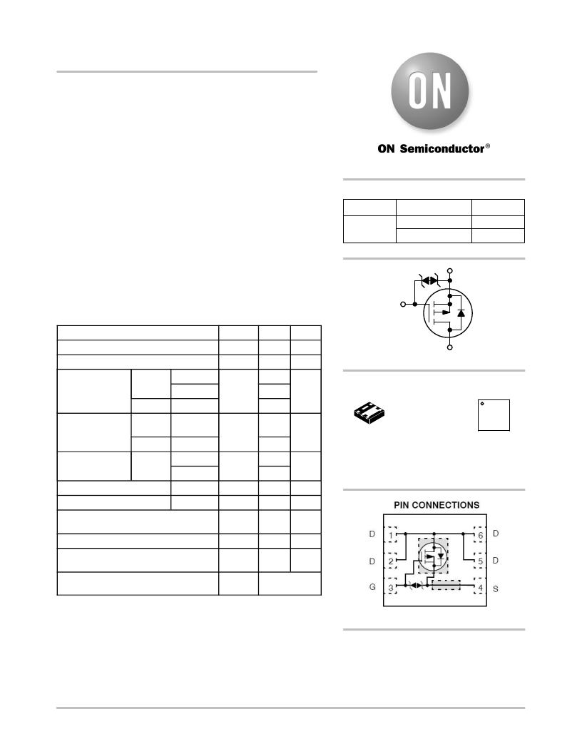
�S�
�G�
�I� D� MAX�
�?� 3.0� A�
�?� 2.0� A�
�MAXIMUM� RATINGS� (T� J� =� 25� °� C� unless� otherwise� stated)�
�Parameter�
�Symbol�
�Value�
�Units�
�Drain-to-Source� Voltage�
�Gate-to-Source� Voltage�
�V� DSS�
�V� GS�
�?� 30�
�±� 20�
�V�
�V�
�D�
�P� ?� Channel� MOSFET�
�Continuous� Drain�
�Current� (Note� 1)�
�Steady�
�State�
�T� A� =� 25� °� C�
�T� A� =� 85� °� C�
�I� D�
�?� 3.0�
�?� 2.3�
�A�
�MARKING�
�DIAGRAM�
�Power� Dissipation�
�(Note� 1)�
�t� ≤� 5s�
�Steady�
�State�
�T� A� =� 25� °� C�
�T� A� =� 25� °� C�
�P� D�
�?� 4.0�
�1.5�
�W�
�1�
�6�
�UDFN6�
�CASE� 517AU�
�m� COOL� t�
�1�
�AC� M� G�
�G�
�t� ≤� 5s�
�T� A� =� 25� °� C�
�2.3�
�AC� =� Specific� Device� Code�
�Continuous� Drain�
�Current� (Note� 2)�
�Steady�
�State�
�T� A� =� 25� °� C�
�T� A� =� 85� °� C�
�I� D�
�?� 2.0�
�?� 1.5�
�A�
�M� =� Date� Code�
�G� =� Pb� ?� Free� Package�
�(Note:� Microdot� may� be� in� either� location)�
�Power� Dissipation� (Note� 2)�
�Pulsed� Drain� Current�
�T� A� =� 25� °� C�
�tp� =� 10� m� s�
�P� D�
�I� DM�
�0.6�
�?� 17�
�W�
�A�
�Operating� Junction� and� Storage�
�Temperature�
�Source� Current� (Body� Diode)� (Note� 2)�
�Lead� Temperature� for� Soldering� Purposes�
�(1/8� ″� from� case� for� 10� s)�
�T� J� ,�
�T� STG�
�I� S�
�T� L�
�-55� to�
�150�
�?� 1.0�
�260�
�°� C�
�A�
�°� C�
�Gate-to-Source� ESD� Rating�
�(HBM)� per� JESD22� ?� A114F�
�ESD�
�Class� 1B�
�Stresses� exceeding� Maximum� Ratings� may� damage� the� device.� Maximum�
�Ratings� are� stress� ratings� only.� Functional� operation� above� the� Recommended�
�Operating� Conditions� is� not� implied.� Extended� exposure� to� stresses� above� the�
�Recommended� Operating� Conditions� may� affect� device� reliability.�
�1.� Surface� Mounted� on� FR4� Board� using� 1� in� sq� pad� size� (Cu� area� =� 1.127� in� sq�
�[2� oz]� including� traces).�
�2.� Surface-mounted� on� FR4� board� using� the� minimum� recommended� pad� size�
�of� 30� mm� 2� ,� 2� oz.� Cu.�
�(Top� View)�
�ORDERING� INFORMATION�
�See� detailed� ordering� and� shipping� information� in� the� package�
�dimensions� section� on� page� 5� of� this� data� sheet.�
�?� Semiconductor� Components� Industries,� LLC,� 2009�
�June,� 2009� ?� Rev.� 0�
�1�
�Publication� Order� Number:�
�NTLUS4195PZ/D�
�发布紧急采购,3分钟左右您将得到回复。
相关PDF资料
NTMD2C02R2SG
MOSFET N/P-CH COMPL 20V 8-SOIC
NTMD2P01R2G
MOSFET PWR P-CHAN DUAL 16V 8SOIC
NTMD4184PFR2G
MOSFET P-CH 30V 2.3A 8-SOIC
NTMD4820NR2G
MOSFET N-CH DUAL 30V 4.9A 8-SOIC
NTMD4840NR2G
MOSFET N-CH DUAL 30V 4.5A 8-SOIC
NTMD4884NFR2G
MOSFET N-CH 30V 3.3A 8-SOIC
NTMD5836NLR2G
MOSFET N-CH 40V 11A SO-8FL
NTMD5838NLR2G
MOSFET N-CH 40V 8.9A 8SOIC
相关代理商/技术参数
NTLUS4930N
制造商:ONSEMI 制造商全称:ON Semiconductor 功能描述:Power MOSFET 30 V, 6.1 A, Single Na??Channel, 2.0x2.0x0.55 mm Cool UDFN6 Package
NTLUS4930NTAG
制造商:ON Semiconductor 功能描述:NFET UDFN6 30V 6.3A 26.3M - Tape and Reel 制造商:ON Semiconductor 功能描述:30V,6.3A,N-Channel power MOSFET
NTLUS4930NTBG
制造商:ON Semiconductor 功能描述:NFET UDFN6 30V 6.3A 26.3M - Tape and Reel
NTLUS4C12N
制造商:ONSEMI 制造商全称:ON Semiconductor 功能描述:Power MOSFET
NTLUS4C12NTAG
制造商:ONSEMI 制造商全称:ON Semiconductor 功能描述:Power MOSFET
NTLUS4C12NTBG
制造商:ONSEMI 制造商全称:ON Semiconductor 功能描述:Power MOSFET
NTM.47M400V
制造商:NIC Components Corp 功能描述:
NTM1
功能描述:电源变压器 TRANSFRMER MIC INPUT PCB VERT 1:1 RATIO
RoHS:否 制造商:Triad Magnetics 功率额定值:12 VA 初级电压额定值:115 V / 230 V 次级电压额定值:12 V / 24 V 安装风格:SMD/SMT 一次绕组:Dual Primary Winding 二次绕组:Dual Secondary Winding 长度:2.5 in 宽度:2 in 高度:1.062 in